1 Overview
The idea of implementing DPSK modulation on the AD9361 is as follows: first verify the spectrum after DPSK modulation in Matlab, then use a pseudo-random sequence as the original data in the FPGA, and send it to the AD9361 after upsampling, shape filtering, and the AD9361 completes the IQ modulated and ultimately emitted. In this article, the final modulated DPSK signal has a physical layer rate of 2Mbps and an occupied bandwidth of 2.5MHz. The physical layer and occupied bandwidth are related.
2. Implementation of DPSK in Matlab
Readin the random sequence generated in the article “Research and Design of Shaping Filters“, perform 4 times upsampling, and then use the filter function to perform shape filtering on the upsampled sequence. The filter coefficients are also generated in “Research and Design of Shaping Filters” , the output data after shape filtering are multiplied with the carrier to obtain the DPSK modulated signal, and finally the spectrum of the DPSK modulated signal is drawn. The Matlab code is as follows:
clear;clc;
ps=1*10^6; %symbol rate is 1Mbps
Fs=4*10^6; %sample rate is 4MHz
fc=1*10^6; %carrier frequncy is 1MHz
N=20000; %lenth of simulation data

coe_int=importdata('D:\Temp\matlab\coe_int.txt');

s=importdata('D:\Temp\matlab\rand_data.txt');

t=0:1/Fs:(N*Fs/ps-1)/Fs; %generate a time series of length N and frequency fs

%sample at Fs frequency
Ads=upsample(s',Fs/ps);

rcos_Ads=filter(coe_int,1,Ads);

%generate carrier frequency signal
f0=sin(2*pi*fc*t);
%generate DPSK modulated signal
dpsk=rcos_Ads.*f0;

%plot the shaped filtered signal spectrum, DPSK signal spectrum, and DPSK signal time domain waveform
m_dpsk=20*log10(abs(fft(dpsk,1024)));
m_dpsk=m_dpsk-max(m_dpsk);
%m_dpsk=mean(m_dpsk,1);

%set the abscissa unit of the amplitude-frequency response to MHz
x_f=[0:(Fs/length(m_dpsk)):Fs/2];x_f=x_f/10^6;

%only the amplitude-frequency response of the positive frequency part is displayed.
mdpsk=m_dpsk(1:length(x_f));

plot(x_f,mdpsk);
legend('DPSK modulated signal spectrum');
xlabel('Frequncy(MHz)');ylabel('Amplituide(dB)');grid on;
The finally drawn DPSK modulated signal spectrum is as shown below. It can be seen that the signal spectrum is limited to about 1.25MHz, which is consistent with expectations.

3. FPGA generates pseudo-random sequence
This code is used to generate pseudo-random sequence as a source in FPGA. In fact, it is impossible to actually generate random sequence in FPGA, but the period of the sequence is very long. One thing to note is that the digital sequence used for DPSK modulation must be random, otherwise separate peaks will appear in the spectrum. The clock rate of the pseudo-random number module is 2MHz. code show as below:
module pn2(clk,rst,data_out);
input clk;
input rst;
output data_out;
reg [7:1] c;
//reg[15:0] cnt;

always @(posedge clk)
begin
if (rst==0)
begin
c<=8'b1010111;
end
else
begin
c[2]<=c[1];
c[3]<=c[2];
c[4]<=c[3];
c[5]<=c[4];
c[6]<=c[5];
c[7]<=c[6];
c[1]<=c[2]^c[3]^c[4]^c[7];
end
end
assign data_out = c[7];
endmodule
4. Constellation mapping
Constellation mapping is actually a simple combinational logic. In the article “Understanding Digital Baseband Signals”, it has been explained that a sequence of -1 1 should be used to replace the 0 1 sequence, so the random 0 1 sequence generated by the FPGA needs to be changed into random -1 1 sequence, here, the usual two’s complement is used to represent -1 to facilitate docking with other modules. The code for constellation mapping is as follows:
module code_convert(
input code_convert_clk,
input code_convert_din,
input code_convert_rst,
output [7:0] dout
);

reg pre_code;
reg pre_code_temp;
reg [7:0] code_convert_dout;

always @(posedge code_convert_clk)
begin
if(code_convert_rst==0)
pre_code_temp <= code_convert_din;
else
begin
if (code_convert_din == pre_code_temp)
begin
code_convert_dout=8'b11111111; //Change to bi-polar code -1.
pre_code_temp <= 1'b0;
end
else
begin
code_convert_dout=8'b00000001; //Change to bi-polar code +1.
pre_code_temp <= 1'b1;
end
end
end

assign dout=code_convert_dout;

endmodule
5. Upsampling and shape filtering
This part can directly use Vivado’s FIR IP core, configure it in 4x interpolation mode, and use the filter coefficients generated in the article “Research and Design of Shaped Filters”, as shown below
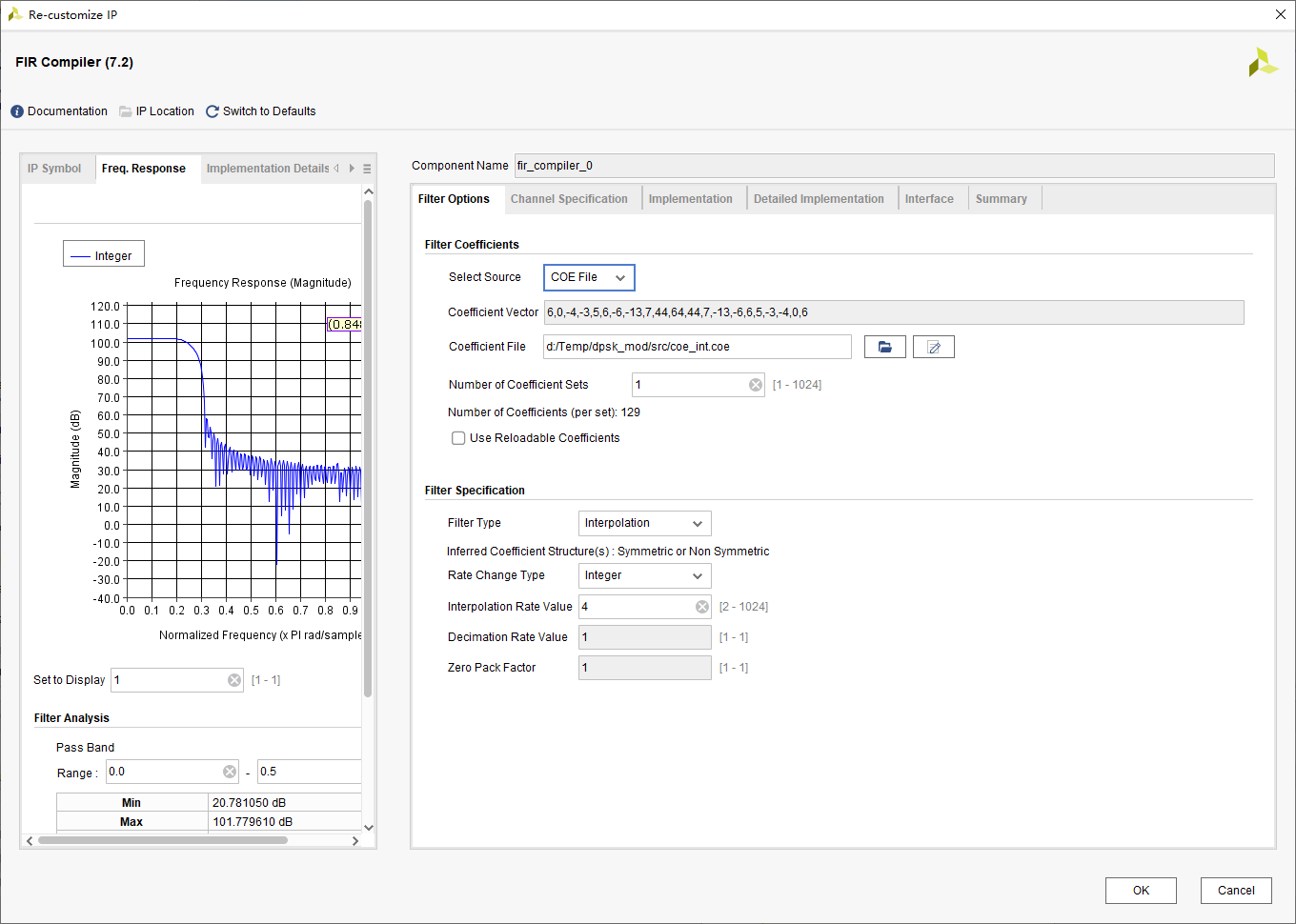
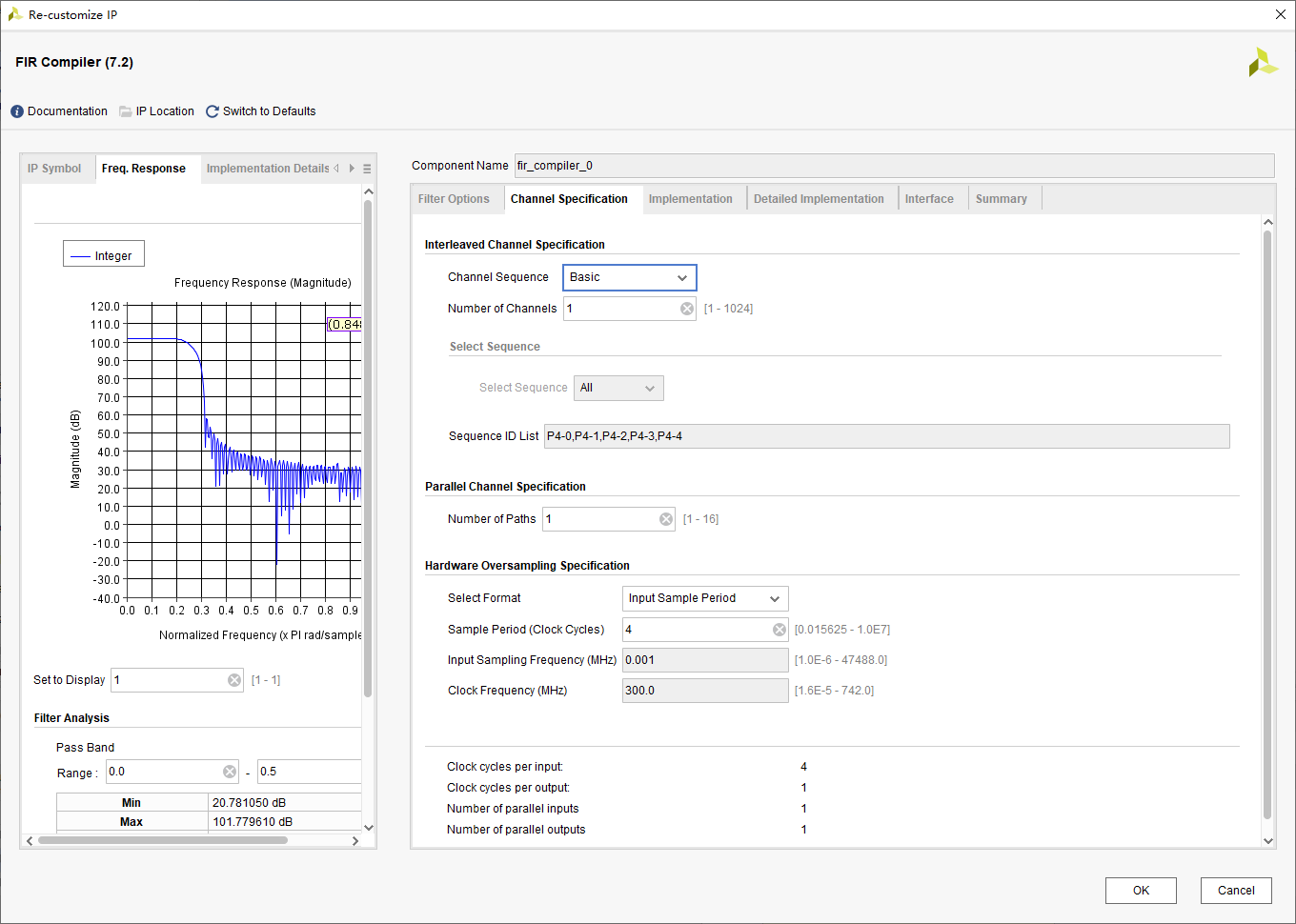
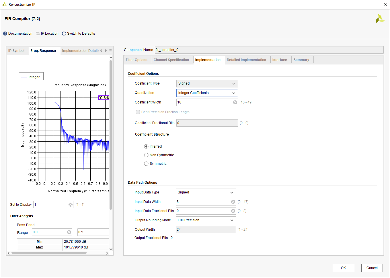
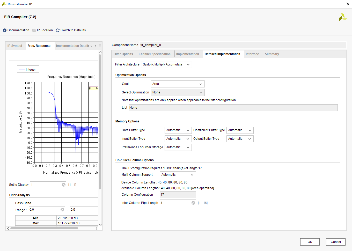
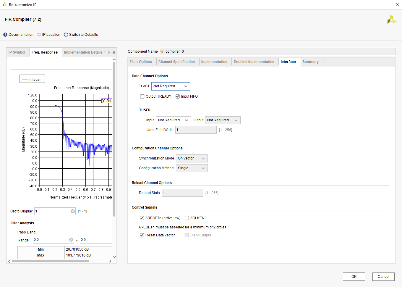
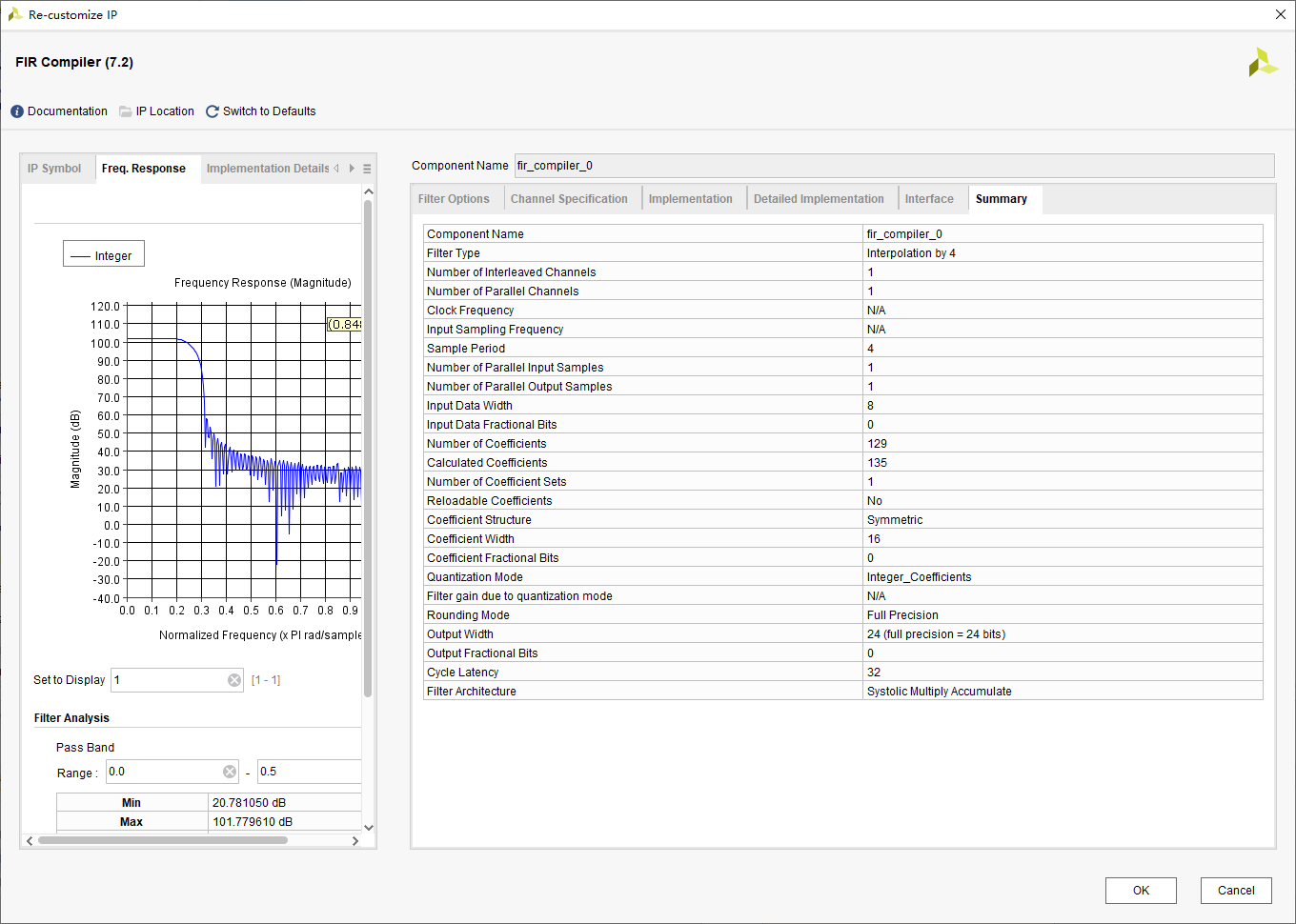
Here we take a look at the changes in data rate. The rate of the original digital sequence is 2Mbps. After constellation mapping, it is still 2Mbps. However, after 4 times the interpolation of the FIR, the rate becomes 8Mbps. Since the FIR interpolation is all 0, the input terminal of the FIR cannot be enabled when the input is 0, so there is a very important operation here, which is to ensure that the input terminal of the FIR is driven by the 8MHz clock and the m_tvalid signal of the FIR is enabled every 4 clock cycles, so as to ensure the correctness of the results. code show as below:
reg [1:0] axis_cnt=0;
always @(posedge clk_8m)
begin
if(!Hard_rstn)
axis_cnt <= 'd0;
else if(s_data_tvalid)
axis_cnt <= axis_cnt + 1'b1;
end

wire m_tvalid;
assign m_tvalid = (s_data_tvalid==1'b1) && (axis_cnt==3'd3);
6. Configuration of AD9361
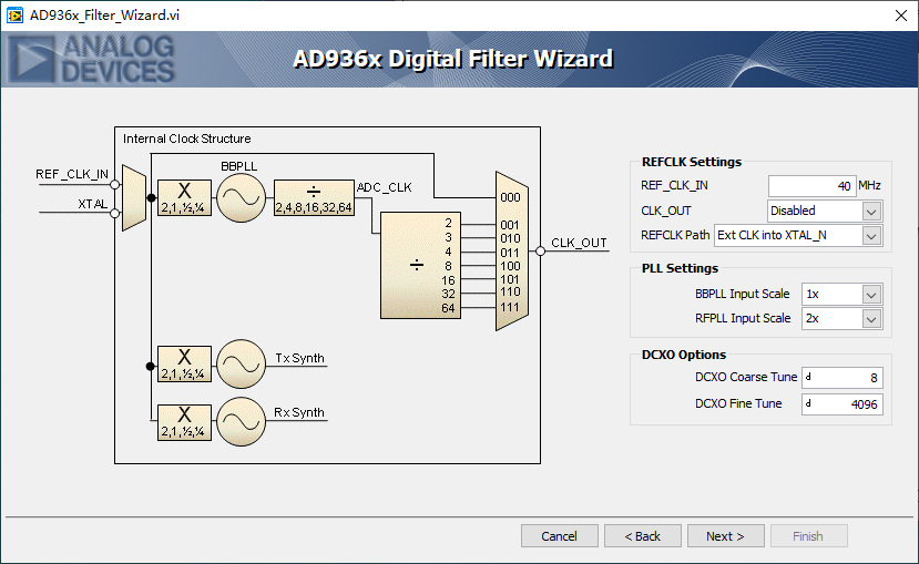
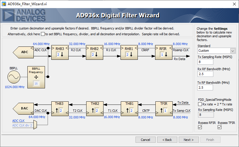
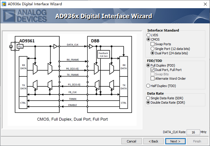
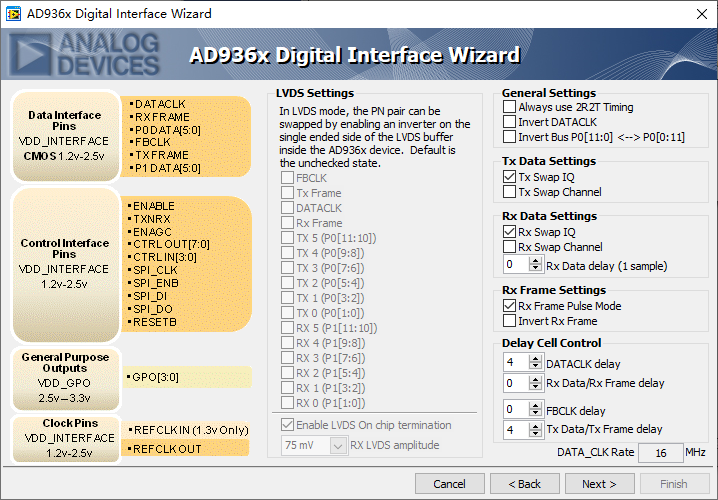
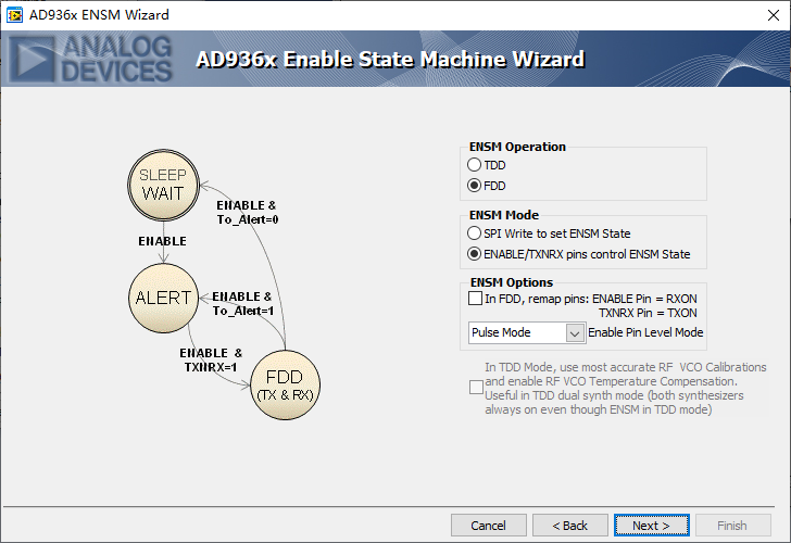
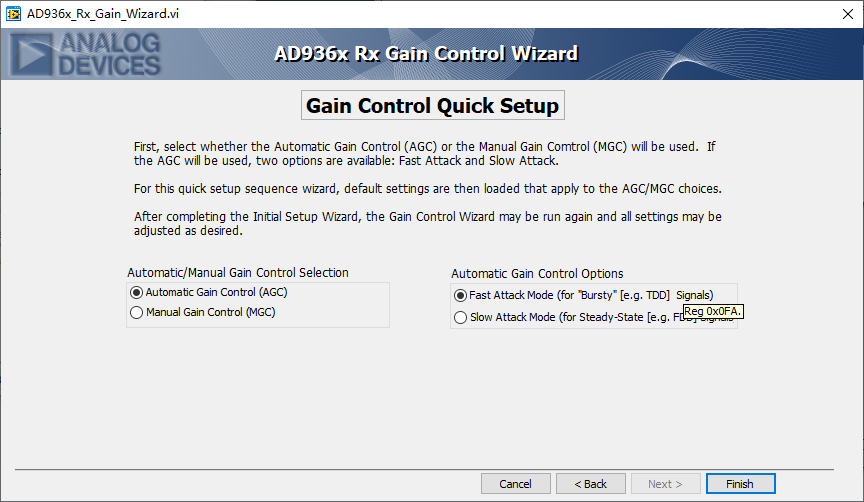
We all know that there are more than 2,000 registers inside AD9361, which is very cumbersome to configure. Using ADI’s official software can simplify the operation. The configuration process of this part focuses on the filter inside the AD9361, as shown in the figure below.

Each transmit channel of AD9361 integrates 4 digital filters including 1 programmable FIR filter and 3 half-band filters. AD9361 also integrates 2 programmable analog filters. Since the shaping filter in this article is implemented on an FPGA, the FIR filter of the AD9361 needs to be bypassed. The next three half-band filters are used normally, and the two analog filters are also configured normally. The configuration process is as follows:


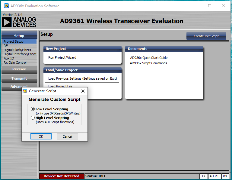
After generating the initialization script, use convert.exe software to convert the script into verilog code, as shown below

In this article, the FPGA uses mormal IO to simulate SPI interface to configure the AD9361. ADI also provides no-OS code, which can be transplanted to the microcontroller or the soft core of the FPGA, so the description will not be carried out here.
There are two other points worth considering: the output of FIR is directly sent to AD9361, and the bit width does not match. You can directly output the high 12 bits of FIR to AD9361. After all, the low-bit data has little impact; DPSK mode, IQ branch just use one channel. In the code of this article, the I channel corresponds to the high 12 bits of the FIR output, and the Q channel is always 0. code show as below:
assign tx_i_ch1=srrc_out[16:5];
assign tx_q_ch1=12'b0;
assign tx_i_ch2=srrc_out[16:5];
assign tx_q_ch2=12'b0;
At this point, all functional modules of DPSK modulation have been completed, as shown below:

Use Vivado to compile the complete project and write the final bitstream file to the FPGA. You can see the expected waveform on the spectrum analyzer, as shown below.
