Network equipment must be inseparable from MAC and PHY. Where there are MAC and PHY, there are corresponding interfaces. Whether visible or invisible, it is there. In Ethernet, this interface is the media independent interface, which is called Media Independent Interface in English, or MII for short. MII is suitable for 100M network equipment. One big disadvantage is that there are a lot of wires, so RMII, or Reduced Media Independent Interface, appeared, which reduced the number of data lines by half based on MII. The birth of Gigabit Ethernet brought about GMII, the Gigabit Media Independent Interface. People found that GMII also had a lot of wiring, so RGMII, the Reduced Gigabit Media Independent Interface, appeared, which is the protagonist of this article. Of course, there is also a serial MII interface family. Readers are asked to consult the relevant literature themselves.
Why RGMII?
There are so many forms of MII interfaces, why did I choose RGMII? The reason is simple: it's wideley used. With the improvement of chip integration, many network processors/SoCs integrate 100M Ethernet switches. If users need to implement a Gigabit Ethernet network, they often need a Gigabit Ethernet PHY with the RGMII interface.
RGMII technical characteristics
As mentioned before, the RGMII interface reduces the number of traces between the MAC and PHY, which is achieved by simultaneous sampling and signal multiplexing on the rising/falling edges of the reference clock. RGMII has two modes: RTBI and RGMII. Since I've never been exposed to RTBI at work, I will not introduce them. RGMII has the following characteristics:
- Compared with the GMII interface, the number of transmit/receive data lines is reduced from 8 to 4
- TX_ER and TX_EN are multiplexed and transmitted through TX_CTL
- RX_ER is multiplexed with RX_DV and transmitted through RX_CTL
- At 1 Gbit/s rate, the clock frequency is 125MHz
- At 100 Mbit/s, the clock frequency is 25MHz
- At 10 Mbit/s rate, the clock frequency is 2.5MHz
- RGMII version 1.3 requirements: The clock is delayed relative to the data line by 1.5-2ns through PCB traces
- RGMII version 2.0 introduces the function of on-chip delay, which implements clock delay inside the chip
RGMII signal definition
RGMII interface timing
RGMII Layout Guide
With the previous description, I believe readers already have the ideas of RGMII Layout, mainly the following:
- Create 2 equal-length groups, refer to TXC and RXC respectively.
- If the MAC/PHY has an internal clock delay, there is no need to delay the clock line.
- If the MAC/PHY does not have internal clock delay, the clock line needs to be delayed.
The delay of the clock line can be well explained by the following pictures, which respectively correspond to PCB delay, MAC+PHY delay and PHY delay. Of course, the method chosen depends on the MAC/PHY chip used.
The clock frequency of RGMII can reach 125MHz at a rate of 1 Gbit/s. As you can imagine, RGMII Layout also needs to comply with the basic guidelines for high-speed digital circuit wiring:
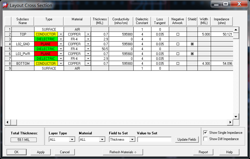
- Impedance control
- 2W/3W principle
Note that in a design where RF and high-speed digital circuits coexist, it is impossible to control the impedance of RF traces and high-speed digital traces at the same time. In this case, be sure to add series matching resistors to all RGMII traces and place them close to the source.
RGMII Layout example
The picture below is a multi-port PHY developed and designed me for a friend, which is connected to the external MAC board through pin headers. Readers must be curious about what this board is used for. In fact, I don’t know either.
Zooming in on one of them, you can see the series matching resistor and winding treatment added by me on the RGMII trace. If you look carefully, you can also see that the trace spacing (Air Gap) is more than 2 times the line width.
View the Constrain Manager and you can see the various settings of RGMII wiring rules.


In fact, the layout method of MII/RMII/GMII is very similar to RGMII, which is left to the readers to explore on their own.


